 Wafer forming process
Achieving ultra-flat wafers with exceptional surface cleanliness
The monocrystalline ingots manufactured by the CZ process go through five carefully controlled steps to become polished wafers.
The five steps of wafer forming
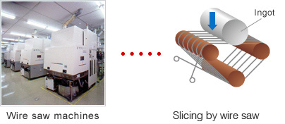
1. Slicing
The circumference of the monocrystalline ingot is ground down to a uniform diameter. Based on the resistivity desired by the customer, the ingot is then cut into slices of around 1mm thickness, using an inner-diameter saw or wire saw, to form the wafers.
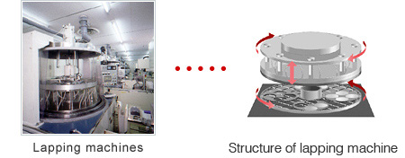
2. Lapping
The sliced wafers are polished by alumina abrasive in a lapping machine to the desired thickness, while improving the surface parallelism.
3. Etching
Mechanical damage to the wafer surface resulting from the earlier steps is removed by chemical etching.
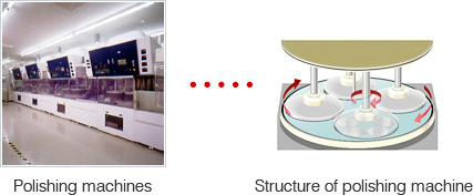
4. Polishing
The wafer surfaces are made perfectly flat and given a mirror finish by means of mechano-chemical polishing using colloidal silica.
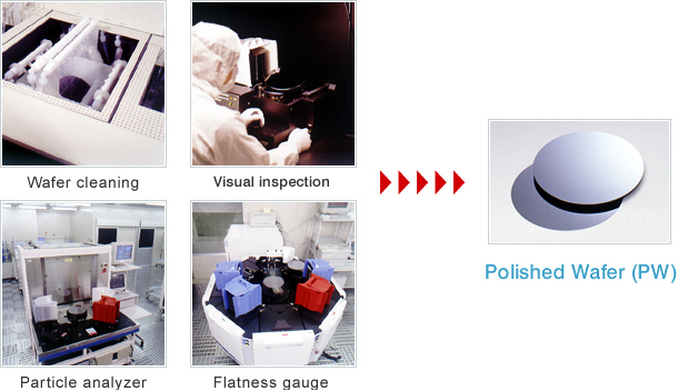
5. Cleaning and inspection
After cleaning, stringent inspections are performed, and the SUMCO polished wafer is completed. The exceptionally high quality of the polished wafers manufactured by SUMCO ensures they are favored by customers all over the world.