Production Processes
Silicon wafers are produced in a highly advanced environment
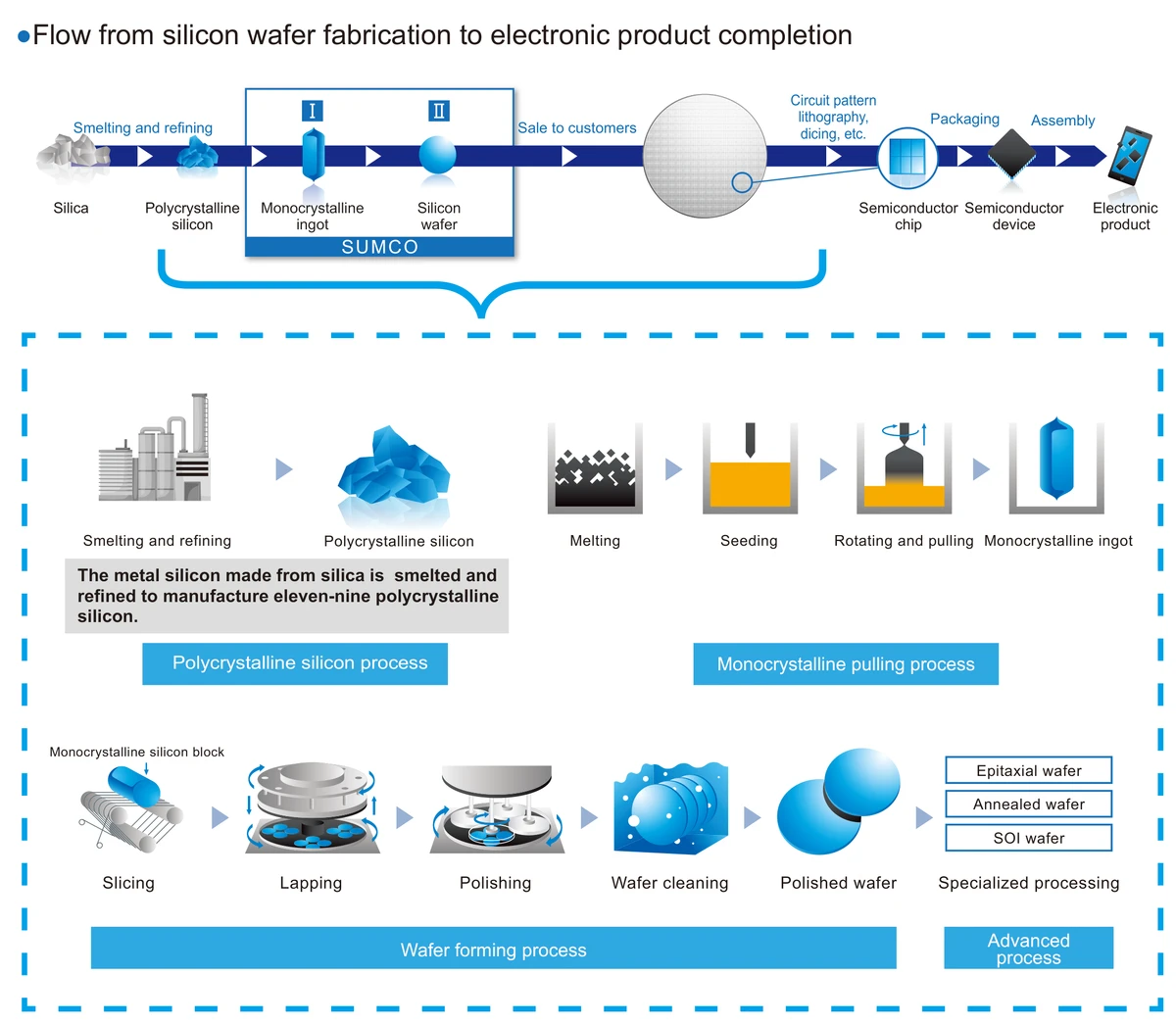
Silicon wafer production takes place in three steps. SUMCO carries out each of these steps in clean rooms boasting the highest level of cleanliness. Applying the strictest quality control, we produce silicon wafers of exceptionally high purity and quality.
Monocrystalline pulling process
Manufacturing of monocrystalline ingots used as the material of silicon wafers
The monocrystalline ingots that make up the silicon wafer are manufactured using high-quality polysilicon as the raw material.
-
Flow of CZ process for making monocrystalline ingot
The monocrystalline silicon ingots from which silicon wafers are created are manufactured by a technique called the CZ (Czochralski) crystal growth process.
Polysilicon purified until the metal impurities are no more than a few parts per billion (ppb) is put into a quartz crucible along with boron (B) and phosphorous (P), and melted at a temperature of around 1420℃. The boron and phosphorous impurities are added in minute amounts to adjust the electrical resistance of the final semiconductors, determining their properties.
A seed crystal silicon rod is placed on the surface of the molten silicon in the crucible, and is pulled up while rotating it, to form a monocrystalline ingot having the same orientation of atoms as the seed crystal. -

Other processes can be used on request
In response to customer needs, we also make use of the MCZ (Magnetic field applied Czochralski) technique, applying a strong magnetic field, or the FZ (Float-Zone) technique whereby monocrystalline ingots are made at low oxygen levels without using a quartz crucible. SUMCO is able to meet customer requests at the monocrystalline ingot manufacturing stage.
Wafer forming process
Achieving ultra-flat wafers with exceptional surface cleanliness
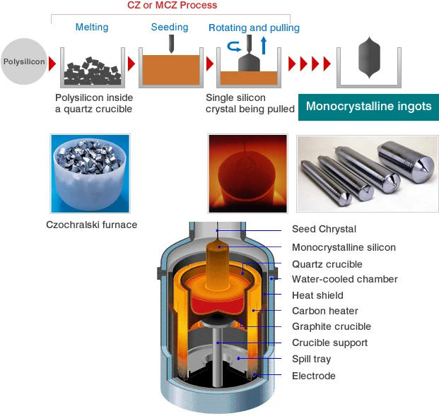
The monocrystalline ingots manufactured by the CZ process go through five carefully controlled steps to become polished wafers.
The five steps of wafer forming
-
01
Slicing
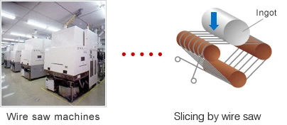
The circumference of the monocrystalline ingot is ground down to a uniform diameter. Based on the resistivity desired by the customer, the ingot is then cut into slices of around 1mm thickness, using an inner-diameter saw or wire saw, to form the wafers.
-
02
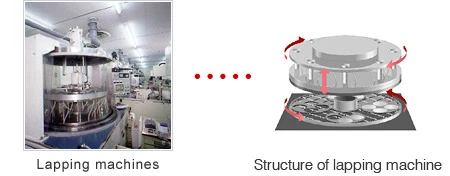
Lapping
The sliced wafers are polished by alumina abrasive in a lapping machine to the desired thickness, while improving the surface parallelism.
-
03
Etching
Mechanical damage to the wafer surface resulting from the earlier steps is removed by chemical etching.
-
04
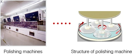
Polishing
The wafer surfaces are made perfectly flat and given a mirror finish by means of mechano-chemical polishing using colloidal silica.
-
05
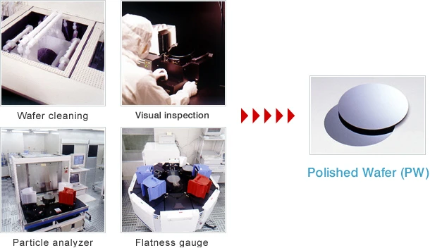
Cleaning and inspection
After cleaning, stringent inspections are performed, and the SUMCO polished wafer is completed. The exceptionally high quality of the polished wafers manufactured by SUMCO ensures they are favored by customers all over the world.
Specialized processing
Specialized wafer processing for specific applications
On request from customers, we perform additional processing on polished wafers, producing the following four kinds of wafers.
Four kinds of specialized processing for specific applications
-
01
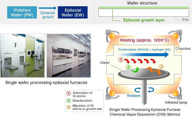
Epitaxial
WafersPolished wafers are heated to around 1200℃ in an epitaxial furnace. Vaporized silicon tetrachloride (SiCl4) and trichlorosilane (SiHCl3) are circulated in the furnace, causing vapor phase (epitaxial) growth of a monocrystalline silicon film on the wafer surface. An epitaxial wafer is a high-quality wafer for customers requiring an exceptionally perfect crystal structure or multiple layers having different resistivity.
-
02
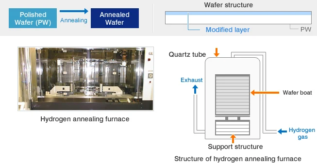
Annealed
WafersA polished wafer undergoes high-temperature annealing in an atmosphere of hydrogen or argon. As this process removes oxygen near the wafer surface, the resulting wafer has improved crystal perfection.
-
03
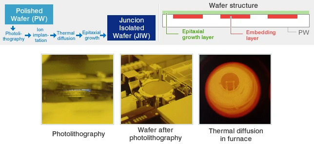
Junction Isolated Wafers
(JIW)Photolithography, ion implantation, and thermal diffusion techniques are used in accordance with customer design needs. After a layer for embedding integrated circuits is formed on the surface, another layer is formed on top of it by epitaxial growth.
-
04
Silicon-On-Insulator
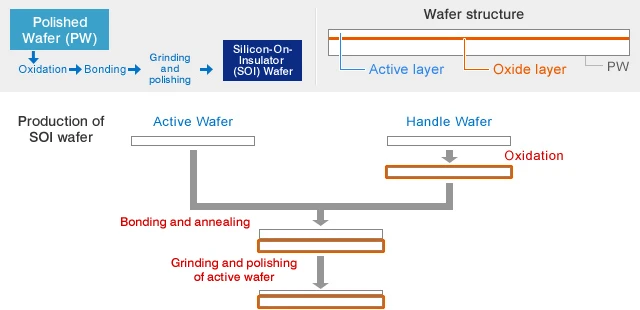
WafersAn oxide layer is formed for one or both of the handle wafer and the active wafer on which semiconductor devices will be built. The two wafers are then bonded together by annealing. Next the active wafer is ground and polished to the desired thickness.
By forming an oxide layer with high electrical insulation inside the wafer, semiconductor devices with high integration, low power consumption, high speed, and high reliability can be realized. A diffusion layer of arsenic (As) or antimony (Sb) can be formed in the active layer as necessary.